- 您现在的位置:买卖IC网 > Sheet目录39246 > LM2576D2TR4-12 (ON SEMICONDUCTOR) 7.5 A SWITCHING REGULATOR, 63 kHz SWITCHING FREQ-MAX, PSSO5
LM2576
http://onsemi.com
8
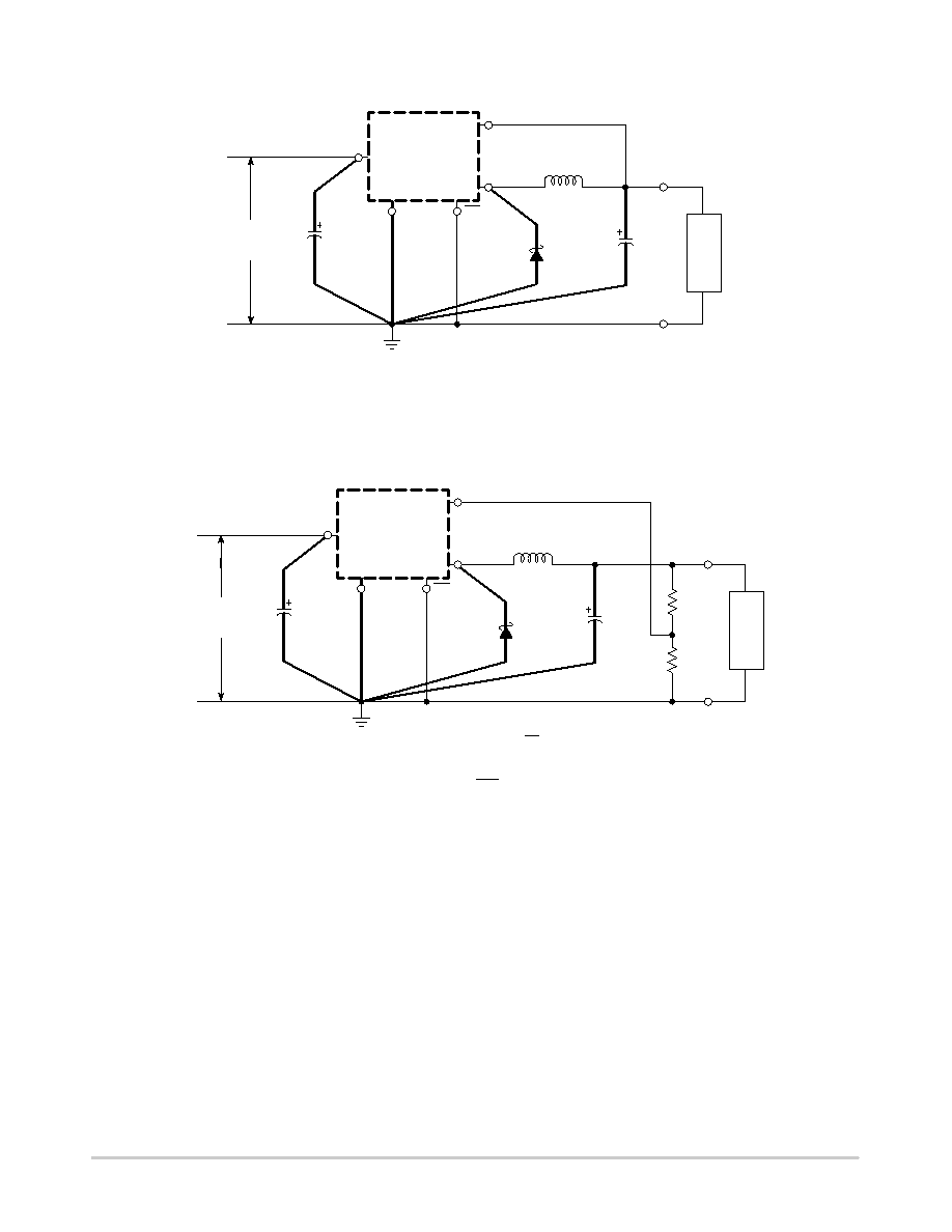
Figure 15. Typical Test Circuit
D1
MBR360
L1
100
mH
Output
2
4
Feedback
Cout
1000
mF
Cin
100
mF
LM2576
Fixed Output
1
5
3ON/OFF
GN
D
Vin
Load
Vout
D1
MBR360
L1
100
mH
Output
2
4
Feedback
Cout
1000
mF
Cin
100
mF
LM2576
Adjustable
1
5
3ON/OFF
GN
D
Vin
Load
Vout
5,000 V
Fixed Output Voltage Versions
Adjustable Output Voltage Versions
Vout + Vref 1.0 )
R2
R1
R2
+ R1
Vout
V
ref
– 1.0
Where Vref = 1.23 V, R1
between 1.0 k and 5.0 k
R2
R1
Cin
100
mF, 75 V, Aluminium Electrolytic
Cout
1000
mF, 25 V, Aluminium Electrolytic
D1
Schottky, MBR360
L1
100
mH, Pulse Eng. PE92108
R1
2.0 k, 0.1%
R2
6.12 k, 0.1%
7.0 V 40 V
Unregulated
DC Input
7.0 V 40 V
Unregulated
DC Input
PCB LAYOUT GUIDELINES
As in any switching regulator, the layout of the printed
circuit board is very important. Rapidly switching currents
associated with wiring inductance, stray capacitance and
parasitic inductance of the printed circuit board traces can
generate
voltage
transients
which
can
generate
electromagnetic interferences (EMI) and affect the desired
operation. As indicated in the Figure 15, to minimize
inductance and ground loops, the length of the leads
indicated by heavy lines should be kept as short as possible.
For best results, singlepoint grounding (as indicated) or
ground plane construction should be used.
On the other hand, the PCB area connected to the Pin 2
(emitter of the internal switch) of the LM2576 should be
kept to a minimum in order to minimize coupling to sensitive
circuitry.
Another sensitive part of the circuit is the feedback. It is
important to keep the sensitive feedback wiring short. To
assure this, physically locate the programming resistors near
to the regulator, when using the adjustable version of the
LM2576 regulator.
发布紧急采购,3分钟左右您将得到回复。
相关PDF资料
LM2576TV-12G
7.5 A SWITCHING REGULATOR, 63 kHz SWITCHING FREQ-MAX, PZFM5
LM2596-12MWC
7.5 A SWITCHING REGULATOR, 173 kHz SWITCHING FREQ-MAX, UUC
LM2596-ADJMWC
7.5 A SWITCHING REGULATOR, 173 kHz SWITCHING FREQ-MAX, UUC
LM2596-ADJMDC
7.5 A SWITCHING REGULATOR, 173 kHz SWITCHING FREQ-MAX, UUC
LM2601MDC
1-CHANNEL POWER SUPPLY SUPPORT CKT, UUC
LM2601MWC
1-CHANNEL POWER SUPPLY SUPPORT CKT, UUC
LM2636MTC/NOPB
SWITCHING CONTROLLER, 2000 kHz SWITCHING FREQ-MAX, PDSO20
LM2636M/NOPB
SWITCHING CONTROLLER, 2000 kHz SWITCHING FREQ-MAX, PDSO20
相关代理商/技术参数
LM2576D2TR4-3.3
功能描述:直流/直流开关调节器 3.3V 3A Buck PWM RoHS:否 制造商:International Rectifier 最大输入电压:21 V 开关频率:1.5 MHz 输出电压:0.5 V to 0.86 V 输出电流:4 A 输出端数量: 最大工作温度: 安装风格:SMD/SMT 封装 / 箱体:PQFN 4 x 5
LM2576D2TR4-3.3G
功能描述:直流/直流开关调节器 3.3V 3A Buck PWM RoHS:否 制造商:International Rectifier 最大输入电压:21 V 开关频率:1.5 MHz 输出电压:0.5 V to 0.86 V 输出电流:4 A 输出端数量: 最大工作温度: 安装风格:SMD/SMT 封装 / 箱体:PQFN 4 x 5
LM2576D2TR4-3.3G-CUT TAPE
制造商:ON 功能描述:LM2576 Series 40 V 3 A 52 kHz Step-Down Switching Regulator - D2PAK-5
LM2576D2TR4-5G
功能描述:直流/直流开关调节器 5V 3A Buck PWM RoHS:否 制造商:International Rectifier 最大输入电压:21 V 开关频率:1.5 MHz 输出电压:0.5 V to 0.86 V 输出电流:4 A 输出端数量: 最大工作温度: 安装风格:SMD/SMT 封装 / 箱体:PQFN 4 x 5
LM2576DP-12
制造商:HTC 制造商全称:HTC Korea TAEJIN Technology Co. 功能描述:3A, 52kHz, Step-Down Switching Regulator
LM2576DP-3.3
制造商:HTC 制造商全称:HTC Korea TAEJIN Technology Co. 功能描述:3A, 52kHz, Step-Down Switching Regulator
LM2576DP-5.0
制造商:HTC 制造商全称:HTC Korea TAEJIN Technology Co. 功能描述:3A, 52kHz, Step-Down Switching Regulator
LM2576DP-ADJ
制造商:HTC 制造商全称:HTC Korea TAEJIN Technology Co. 功能描述:3A, 52kHz, Step-Down Switching Regulator